8-bit Small Package QG MCUs
The S08QG Family of microcontrollers provide a wide variety of serial interfaces and peripherals, normally found in higher-end devices, all in a small package. Featuring low-power S08 8-bit architecture, S08QG devices are a good fit for battery-powered devices.
产品详情
Features
8-bit HCS08 Central Processing Unit (CPU)
- Up to 20 MHz HCS08 CPU (10 MHz bus frequency) for 100 ns minimum instruction time
- HCS08 instruction set with added BGND instruction
- Support for up to 32 interrupt/reset sources
Integrated Third-Generation Flash Memory and RAM
- Embedded flash that is in-application reprogrammable
- Extremely fast, byte-writable programming (20 µs/byte)
- Up to 100,000 write/erase cycles at typical voltage and temperature (10k minimum write/erase)
- 100 years typical data retention (15 years minimum)
Flexible Clock Options
- Internal clock source (ICS) module containing a frequency-locked loop (FLL) controlled by internal or external reference
- Precision trimming of internal reference allows typical 0.1 percent resolution and +0.5 percent to -1 percent deviation over operating temperature and voltage
- Internal reference can be trimmed from 31.25 kHz to 39.065 kHz, allowing for 8 MHz to 10 MHz FLL output
- Low-power oscillator module (XOSC) with software selectable crystal or ceramic resonator range, 31.25 kHz to 38.4 kHz or 1MHz to 16 MHz, and supports external clock source input up to 20 MHz
Input/Output
- 12 Bidirectional Input/Output (I/O) Lines
- One Input Only and One Output Only Line
- Outputs 10 mA each; 60 mA max for package
- Software selectable pull-ups on ports when used as input
- internal pull-up on reset and interrupt request (IRQ) pin
- Software selectable slew rate control and drive strength on ports when used as output
- 8-pin keyboard interrupt module with software selectable polarity on edge or edge/level modes
Integrated Analog Peripherals
- 8-ch., 10-bit analog-to-digital converter (ADC)
- Automatic compare function, software programmable for greater than/equal to or less than conditions
- Asynchronous clock source
- Temperature sensor
- Internal bandgap reference channel
- Hardware triggerable using the RTI counter
- Low-power and high-speed options
- Analog comparator module (ACMP)
- Option to compare to internal reference
- Option to route comparator output directly to pin
- Output can be optionally routed to TPM module as input capture trigger
Two Timer Modules
- Programmable 16-bit timer/PWM module (TPM)
- 8-bit modulo timer module (MTIM) with 8-bit prescaler
System Protection
- Watchdog computer operating properly (COP) reset with option to run from dedicated 1 kHz internal clock source or bus clock
- Low-voltage detection with reset or interrupt
- Illegal op code detection with reset
- Flash block protection
- Security feature for flash and RAM
- Always-on power-on reset (POR) circuitry
Development Support
- On-chip ICE
Multiple Serial Communication Options
- Serial communications interface module
- Option for 13-bit break capabilities
- Double-buffered transmit and receive
- Serial peripheral interface module
- I²C bus module
购买/参数
|
|
|
|
|
|
|
|---|---|---|---|---|---|
|
|
|
|
|
|
|
|
|
|
|
|
|
|
|
|
|
|
|
|
|
|
|
|
|
|
|
|
|
|
|
|
|
|
|
|
|
|
|
|
|
|
|
|
|
|
|
|
|
|
|
|
|
|
|
|
|
|
|
|
|
|
|
|
|
|
|
|
|
|
文档
快速参考恩智浦 文档类别.
设计资源
硬件
1-5 / 7 硬件
-
 仿真器、探测器、编程器
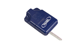
Universal Multilink开发接口亮点
-
 评估板和开发板
MC9S08QG8 Demonstration Board 亮点
-
 仿真器、探测器、编程器
PEmicro Cyclone编程器
-
 仿真器、探测器、编程器
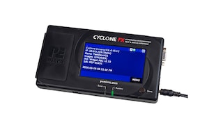
PEmicro Cyclone FX编程器
-
 仿真器、探测器、编程器
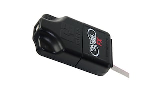
Universal Multilink FX高速开发接口
软件
快速参考恩智浦 软件类型.
1-5 / 14 软件文件
-
BSP及设备驱动
NXP eGUI: Graphical LCD Driver for MCUs/MPUs亮点
-
可访问其他软件。 查看我们的精选合作伙伴解决方案.
注意: 推荐在电脑端下载软件,体验更佳。
工程服务
如需恩智浦直接支持,请参阅 工程服务.
1 工程服务
-
独立设计公司(IDH)
Hardware/Software Engineering Services
要查找支持该产品的其他合作伙伴产品,请访问我们的 合作伙伴市场.


