高压USB PD电源开关
设计文件

收到完整的详细信息。 请参阅 eCad 文件中的产品足迹等。
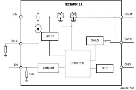
The NX30P0121UK is an advanced 3 A power switch. It includes UnderVoltage LockOut (UVLO), VOUT OverVoltage LockOut (OVLO), OVLO adjustable pin, and over-temperature protection circuits. It is designed to automatically isolate the power switch terminals when a fault condition occurs. Both VIN and VOUT pins have 29 V tolerance in shutdown mode.
The device has a default internal 14.5 V overvoltage protection threshold in VOUT and adjustable OVP threshold by resistor divider from VOUT. ISNS pin is current source output proportional to input current from VIN to VOUT when the device is enabled.
The device is enabled by external EN pin. When EN pin is driven LOW, the device is in shutdown mode where all internal circuitries are off and OVP switch is off. When EN pin is driven HIGH and VIN is valid, the OVP switch soft starts after VIN debounce time to limit the inrush current.
NX30P0121UK is offered in a small 12 bumps, 1.65 x 1.25 x 0.525 mm WLCSP package.
高压USB PD电源开关
1 结果
包含 0 不推荐用于新设计
部件 | 订购 | 计算机辅助设计模型 | Application Voltage (V) | 渠道 | 状态 | 预算报价(不含税) | 封装类型 | 输入电压[最小到最大](V) | VDC Absolute (Max) (V) | Isw (A) | RDSon (mohm) |
|---|---|---|---|---|---|---|---|---|---|---|---|
20 | 1 x VBUS | 正常供应 | 1K @ CNY4.45 | WLCSP12 | 2.5 to 20 | 29 | 3 | 54 |
快速参考恩智浦 文档类别.
3 文件
紧凑列表
3 文件
紧凑列表
收到完整的详细信息。 请参阅 eCad 文件中的产品足迹等。
There are no recently viewed products to display.