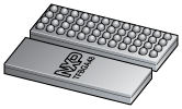
12-Bit Bus Switch/Multiplexer for DDR4-DDR3-DDR2 Applications
- 本页面包含有关样品阶段产品的信息。此处的规格和信息如有更改,恕不另行通知。如需了解其他信息,请联系支持人员或您的销售代表。
The CBTV24DD12 is designed for 1.8 V / 2.5 V / 3.3 V supply voltage operation and it supports Pseudo Open Drain (POD), SSTL_12, SSTL_15 or SSTL_18 signaling and CMOS select input levels. This device is designed for operation in DDR4, DDR3 or DDR2 memory bus systems, with speeds up to 3200 MT/s.
The CBTV24DD12 has a 1:2 switch or 2:1 multiplex topology and offers a 12-bit wide bus. Each 12-bit wide A-port can be switched to one of two ports B and C, for all bits simultaneously. Each port is non-directional due to the use of FET switches, allowing a multitude of applications requiring high-bandwidth switching or multiplexing.
The selection of the port is by a simple CMOS input (SELect). Another CMOS input (ENable) is available to allow all ports to be disconnected. The SEL0, SEL1 and EN input signals are designed to operate transparently as CMOS input level signals up to 3.3 V. The CBTV24DD12 uses NXP’s proprietary high-speed switch architecture providing high bandwidth, very little insertion loss, return loss, and very low propagation delay, allowing use in many applications requiring switching or multiplexing of high-speed signals. It is available in a 3.0 mm x 8.0 mm TFBGA48 package with 0.65 mm ball pitch, for optimal size versus board layout density considerations. It is characterized for operation from -10 °C to +85 °C.
产品详情
Features
Topology
- 12-bit bus width
- 1:2 switch/MUX topology
- Bidirectional operation
- Simple CMOS select pins (SEL0, SEL1)
- Simple CMOS enable pin
Performance
- 3200 MT/s throughput
- 7.4 GHz bandwidth (for both single-ended and differential signals)
- Low ON insertion loss
- Low return loss
- Low crosstalk
- High OFF isolation
- POD_12, SSTL_12, SSTL_15 or SSTL_18 signaling
- Low RON (8 Ω typical)
- Low ΔRON (<1 Ω)
General attributes
- 1.8 V / 2.5 V / 3.3 V supply voltage operation
- Very low supply current (600 µA typical)
- Back current protection on all the I/O pins of these switches
- ESD robustness exceeds 2.5 kV HBM, 1 kV CDM
- Available in TFBGA48 package, 3.0 mm × 8.0 mm × 1.0 mm size, 0.65 mm pitch, Pb-free/Dark Green
Target Applications
- DDR4/DDR3/DDR2 memory bus systems
- NVDIMM module
- Systems requiring high-speed multiplexing
- Flash memory array subsystem

