Author

NXP
At NXP, innovation is always now, but our focus is always the future. Our dedicated team of experts is united by a passion to make everyday life more remarkable through technologies that continually redefine life as we know it.

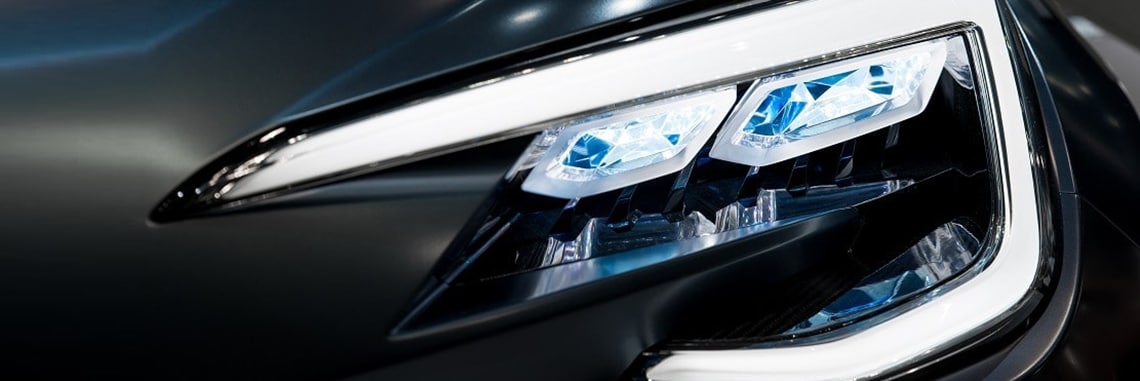
Plenty of ink is given to global trends to make our lives greener, but hidden away is a little gem that I’d like to talk about today. The automotive lighting systems are ripe for innovation and improvement, particularly with the introduction of LED and laser diode technologies a few years ago. LED lamps with a laser channel, usually equipped with Adaptive Front Lighting System (AFS) or matrix beams, are becoming increasingly popular with automakers. This is not just because they save energy, which they do, but also because they are glare-free and extend the light range.
Which is why being able to offer a solution that combines multiple loads more efficiently in a flexible platform is of particular interest to design engineers today.
I’m going to explain how this can be done using the LED headlamp with a laser channel as an example.
Typically, the light control unit (LCU) drives both the laser channel and the Daytime Running Lamp (DRL) channels simultaneously with one boost voltage. This is not very efficient and incurs heat dissipation for the laser channel- since the boost voltage shares a common voltage with DRL, it is higher than is needed to drive the laser channel.
Automotive Solid State Lighting (ASSL) driver ICs can solve this issue by providing two independent voltages that can be controlled individually via a SPI interface, resulting in higher system level efficiency.
The LCU is the key component for a LED headlamp with laser. Its driver module usually contains a microcontroller and transceivers to communicate to the Body Control Module (BCM). The MCU controls the drive IC via the SPI interface; while commands from the BCM or the LCU sense traffic conditions by analyzing signals from cameras or sensors. In power electronics architecture, a two-stage topology is often used. It employs a boost voltage regulator and independent buck channels to drive LEDs or laser diodes for the different lighting functions.
This two stage topology means that there is a stable voltage source for a wide range of conditions, while still responding to dynamic load in each stage. This feature is critical in matrix or full LED headlight designs, since selecting external components for different buck channels could prove to be counterproductive.
For example, buck channels driving DRL have a relatively low output current of 0.2-1.0 A, but a high voltage: so the MOSFET drain-source voltage (VDS) and diode reverse leakage current are important. However, buck channels driving laser channels have a higher output current of > 1.0 A, but a low VF: so the MOSFET drain-source on-state Resistance (Rdson), inductor DC Resistance (DCR) and diode forward voltages are more important.
One voltage would struggle to drive all these channels, so using two boost voltages or one boost voltage and one SEPIC voltage with a controller IC brings a powerful digital regulation loop. Or, in other words, it increases system efficiency by optimizing the buck channel duty cycle and reducing power loss in buck freewheel diode.
This type of flexible platform can combine loads efficiently and deliver on the promise of LED lighting.
You can read more on this topic here.

At NXP, innovation is always now, but our focus is always the future. Our dedicated team of experts is united by a passion to make everyday life more remarkable through technologies that continually redefine life as we know it.

2020年6月19日
by Ross McOuat

2020年7月29日
by Davina Moore

2020年7月30日
by Jason Deal