We’re all familiar with the basic idea of a surface-mount power
component soldered to a PCB, where the primary means of heat removal from
the component is via the PCB itself.
My previous post,
Can we know Tj by looking at Tcase?, considered a configuration exactly like this. It posed the question:
“Can I determine the junction temperature (Tj) of my
MOSFET from its case temperature (Tcase)?” I demonstrated
that, for the
LFPAK56
package, Tj and Tcase are almost identical whether we
consider results from simulation or real-life experiments. At the end of the
blog, I left the reader to ponder why Tj @
Tcase — that is question that I’m returning to
now.
To appreciate why Tj @ Tcase, we need to look at what
happens to the majority of the heat energy when it leaves the component.
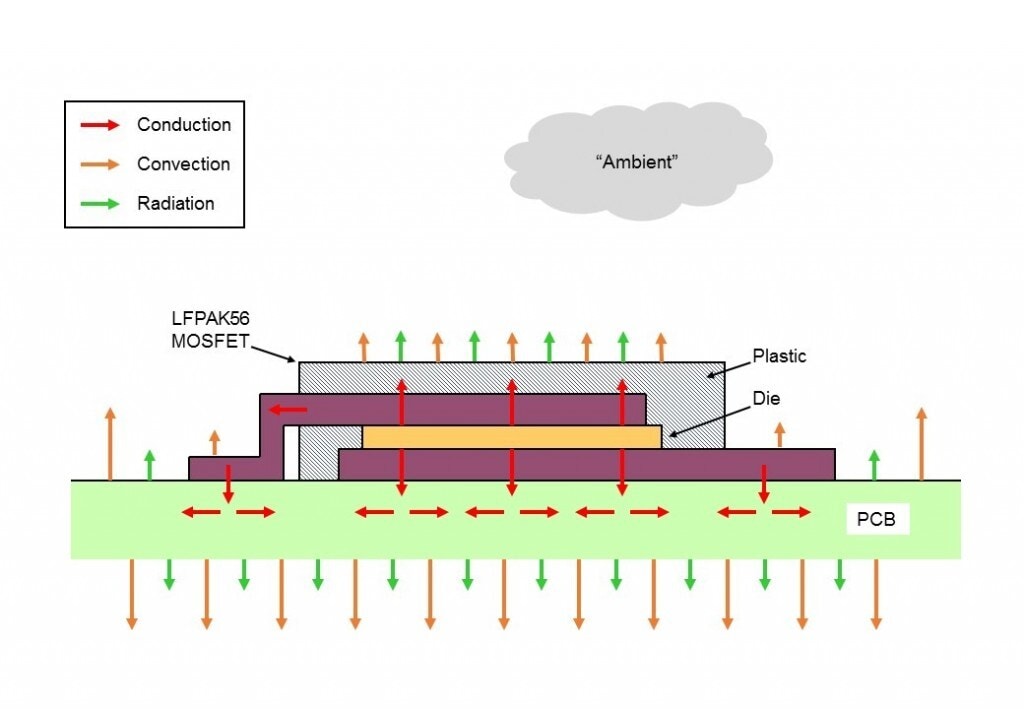
Let’s start by considering the somewhat simplified diagram of an
LFPAK56 MOSFET mounted on a PCB (Figure 1), and its associated heat paths.

Figure 1. A simplified view of an LFPAK56 MOSFET mounted on a PCB and its
associated heat paths to ambient
The heat paths from the MOSFET die to “ambient” are quite easy
to define, but what is happening to the temperature immediately
surrounding the device and PCB? If the die is operating at an elevated
temperature, then intuitively we wouldn’t expect the air temperature
close to the PCB to be at ambient temperature – but what is the
temperature?
This question is actually quite hard to answer in the lab as thermal cameras
tend to see straight through air. Fortunately we can gain some understanding
by running a thermal simulation. See Figure 2. In this case Tamb =
20°C and PD = 1W.

Figure 2. Thermal simulation plots of an LFPAK56 device on a PCB
In Figure 2, we see the surface temperature plot of the PCB and also of a
vertical “slice” through the air surrounding the device and PCB.
I have left the LFPAK56 device itself uncoloured so that you can see it more
easily.
According to the simulation, Tj = 69.5°C and the temperature
of the air flowing upwards from the PCB surface is around 65°C at points
close to the PCB and device. In other words, the device is surrounded by a
blanket of warm air originating from the surface of the PCB which is at a
temperature quite close to Tj. Most of the heating of the case top
surface (Tcase) is therefore due to this surrounding blanket of air
rather than direct heating of the surface by the die underneath. In fact, the
simulation predicts that less the 1% of the total die heat flux is passing out
through the top of the device case!
This result is perhaps another one that we might classify as
“non-intuitive,” but it does go some way to answering our
original question of why Tj @ Tcase. We have to consider
more than just the simple one-dimensional internal heat path from the die to
the top surface of the package.
In my next post, I’ll take a final look at this scenario, and consider
why “thermal resistances” would not have helped us in this
situation.


